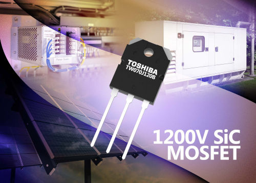
The new TW070J120B power MOSFET is based on SiC, a novel material with a large band gap that enables devices to operate at high voltages, as well as high switching speeds and low on-resistance compared to conventional silicon-based MOSFETs and IGBTs (insulated gate bipolar transistors). As a result, the new MOSFET significantly contributes to reduced power consumption and improved power density, thus opening new opportunities for system downsizing. The new SiC MOSFET
is manufactured using Toshiba's second-generation chip design[1] and offers increased reliability. Furthermore, the TW070J120B achieves a low input capacitance (CISS) of 1680pF (typ.), a low gate input charge (Qg) of 67nC (typ.), and a drain-source on-resistance (RDS(ON)) of only 70 mΩ (typ.).
Compared to a 1200V silicon IGBT like Toshiba's GT40QR21, the new device reduces switching losses by approximately 80% and switching time (fall-off time) by nearly 70%, while also offering low forward voltage characteristics with a drain current (ID) of up to 20A.
The high gate threshold voltage (Vth) (between 4.2V and 5.8V) minimizes the potential for spurious switching. The inclusion of a SiC Schottky barrier diode (SBD) with a low forward voltage (VDSF) of only -1.35V (typ.) further contributes to reduced losses.
The new TW070J120B MOSFET, supplied in a TO-3P(N) package, will enable the design of more efficient power solutions, especially in industrial applications where increased power density will also help reduce equipment size and weight.





- Details
- Category: Other Semiconductors
1200V Silicon Carbide (SiC) MOSFET
Toshiba Electronics Europe GmbH (“Toshiba”) has introduced a 1200V silicon carbide (SiC) MOSFET intended for high-power industrial applications such as 400V AC input AC/DC power supplies, photovoltaic inverters, and bidirectional DC/DC converters for UPS (uninterruptible power supply systems).



Print Magazine

Annual subscription price:
You will receive all 10 editions that are published each year.
social networks
Popular News Electronics




Spanish electronics magazine. Printed for over 25 years.
Spain - Madrid - All rights reserved © Convertronic Professional Spanish Electronics Magazine.